From Silicon to Circuit Board: The Journey of a Memory Chip
Follow a memory chip from design and wafer fab to packaging, testing and your PCB — and learn why lead times, date codes and EOL happen.
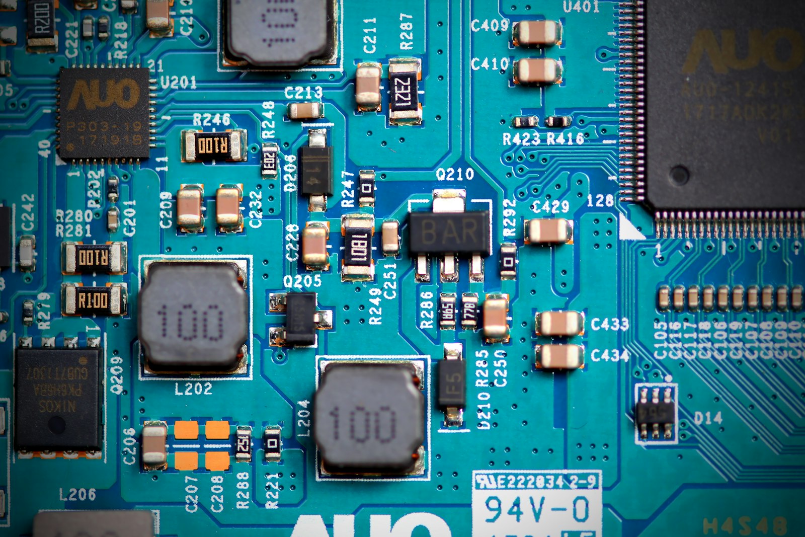
Click “Request Quote” on a distributor’s website, and 5,000 EEPROMs can ship within days. Ask the same memory manufacturer for a fresh production run of that exact part, and you may be quoted 13–26 weeks — sometimes more than a year. The difference is not bureaucracy. It is the journey every chip takes before it can ever appear on a purchase order.
Understanding that journey makes you a sharper buyer. You will know why date codes matter, why parts suddenly go EOL (End of Life), why lead times swing from weeks to quarters, and why two suppliers quoting the same part number can behave so differently. Here is that journey, stage by stage.
Stage 1 — Chip Design: Where Every Memory IC Begins (6–24 Months)
Every memory chip starts life as a specification: density, voltage, interface speed, package, target cost. Design engineers then describe the circuit in hardware description languages such as Verilog or VHDL — a memory design is built from billions of repeated microscopic cells. A DRAM cell is one transistor plus one capacitor; NAND flash stacks charge-storage cells vertically, and leading-edge 3D NAND now climbs past 200 layers per die.

Before anything is manufactured, the design must survive verification — simulation of every operating mode and edge case. Verification typically consumes the majority of a chip project’s total engineering effort. The verified design is then processed by EDA software (from vendors such as Synopsys, Cadence and Siemens EDA), which converts the circuit description into the physical layout of every wire and cell.
The finished layout is sent to the fab in a final handoff called tape-out. At advanced process nodes, the photomask set alone — the glass templates used to print the circuit onto silicon — can cost millions of dollars before a single chip is made.
Stage 2 — Wafer Fabrication: The Three-Month Bottleneck (8–12 Weeks)
Inside a semiconductor fab, hundreds of processed 300 mm silicon wafers move through class-1 cleanrooms on automated vehicles. Building a memory wafer takes well over a thousand process steps — deposition, lithography, etch, ion implantation and planarization, repeated layer after layer — and roughly two to three months of elapsed time. A single wafer yields thousands of individual memory die, which are later sawn apart.
Crucially, fab capacity is not a free market — it is booked. Major customers sign long-term agreements that reserve wafer starts months in advance. When a demand surge hits one product family, the wafers allocated to smaller or older product families do not disappear overnight, but their priority does drop. This is why mainstream memory demand and specialty memory supply are connected even when they use different chips.
Stage 3 — Packaging, Marking and Test (2–4 Weeks)
Sawn die are too fragile to ship, so each one is bonded into a package: die attach, wire bonding or flip-chip connection, then encapsulation in mold compound. After burn-in and final test, parts are graded by speed bin and packed into tape & reel (to the EIA-481 standard), tubes, or JEDEC trays.
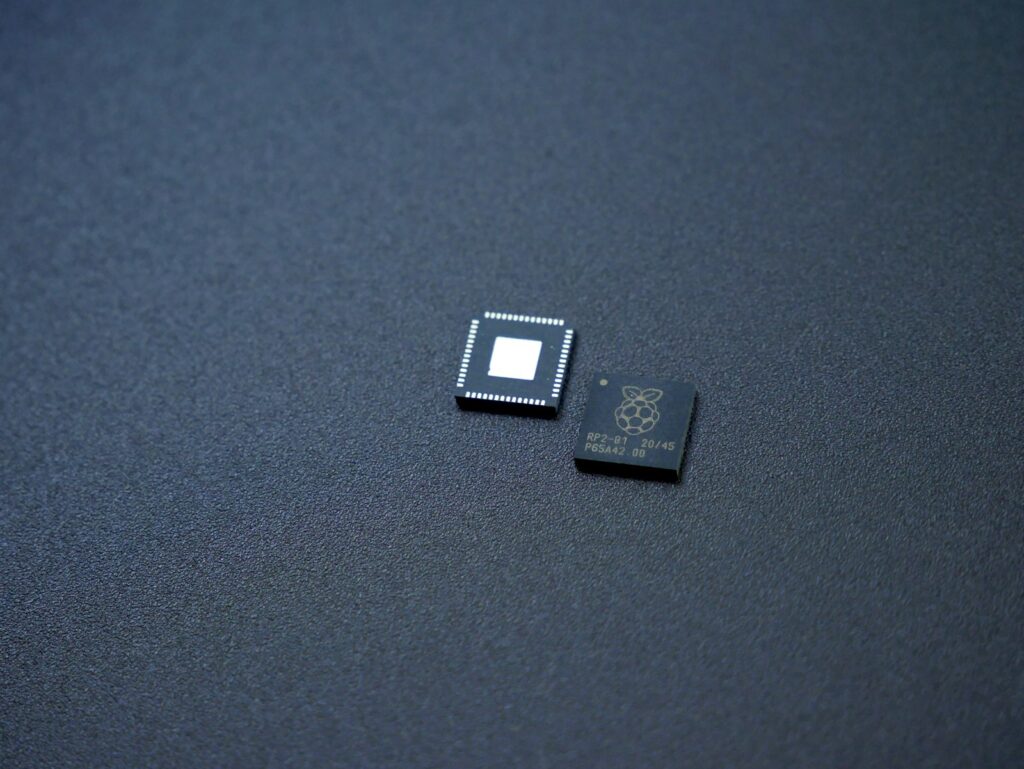
This is also where the package marking you rely on is printed: part number, lot code, and the date code. A date code is four digits — year and week. 2438 means week 38 of 2024. It is the single fastest freshness check a buyer has.
Stage 4 — Distribution: Two Channels, Two Speeds (Days)
Between the manufacturer and your production line sit two kinds of channel. Franchised distributors hold factory contracts and excel at scheduled volume supply of active parts. Independent distributors like us work the open market: spot stock, allocation pressure, allocation excess, and the sourcing of parts that the franchised channel no longer lists — including EOL and hard-to-find components.
For a buyer, the practical difference is what happens when the factory quotes 26 weeks. An independent distributor can often find the same part, properly traceable, available now — which is exactly the gap we exist to fill.
Stage 5 — Landing on Your PCB
The last leg of the journey happens on the SMT line: solder-paste printing, high-speed pick-and-place, and reflow — the board passes through a carefully controlled temperature profile peaking around 245–250 °C for lead-free solder. Before that, opened moisture-sensitive parts must have been stored correctly (dry cabinets, and rebaking per the JEDEC J-STD-033 rules if their floor life expired).
Design-side, a memory IC only behaves if its PCB home is right: decoupling capacitors close to the power pins, clean ground, and matched trace routing for high-speed lines. And through every handling step, ESD discipline — wrist straps, grounded benches, shielded packaging — protects gates that are thinner than the voltage they are exposed to.
What the Journey Means for Your Purchasing Strategy
- Order critical parts with buffer time. Factory-direct lead times are structural, not negotiable — plan around them instead of being surprised by them.
- Watch PCN and EOL feeds for your long-lived designs; the decision that ends a part’s life was made in a roadmap meeting, quarters before you received the notice.
- Check date codes and MSL handling on every receipt — freshness and dry-pack discipline predict how a batch will behave in reflow.
- Qualify a second source before you need one. An emergency is the worst time to be vetting a new supplier.
- When the factory quote is too slow, ask us. Independent sourcing with full traceability, pre-payment video inspection and photo documentation is what we do every day.
Frequently Asked Questions
- How long does it take to make memory chips?
- Once a design exists, roughly 3–4 months of physical production: 8–12 weeks in wafer fabrication plus 2–4 weeks of packaging, test and packing. The design itself takes 6–24 months — and that is before it is ever offered for sale.
- What does the date code on an IC mean?
- Four digits: year and week of assembly. 2438 = week 38 of 2024. It is the quickest way to check stock freshness and traceability before you commit.
- Why do memory chips go end-of-life?
- Because the fab capacity and engineering investment that produced them gets redirected to newer, higher-density or higher-margin products. EOL decisions are economics, not defects — and they are announced in advance via PCN/EOL notices.
- Franchised vs. independent distributor — which do I need?
- Both. Franchised distribution for scheduled volume of active parts; independent distribution when you need stock now, parts that are EOL, or quantities the factory quotes at long lead times. The key on the independent side is documentation: traceability, date codes, and inspection before payment.
- What is MSL and why does it matter?
- Moisture Sensitivity Level — a JEDEC classification of how long a part may sit outside dry packaging before reflow. If exceeded, moisture inside the package can expand during reflow and crack the die. If your parts arrive with the dry-pack seal already broken, ask why.
Need memory chips the factory can’t deliver this quarter?
Every part we ship passes label, date-code and visual inspection, with photos of your exact shipment before dispatch — and video verification is available before you pay.